

“like the children in the game of hot boiled beans and very good butter1, he was warm in his search when he saw the Tower, and cold when he didn’t see it”
- Charles Dicken, The Mystery of Edwin Drood
Two quick asks before we dive deeper:
1. I am in Philadelphia from 8-11th September. If you are a scientist/engineer/founder in the area or know someone who is, hit me up.
2. I am in San Francisco from 12th September onwards. Hit me up then if you are around.
******
At BioCompute, we use solid state nanopores to retrieve data from DNA.
Nanopores (i.e. nano-sized holes on a surface) typically use voltage as a physical property for moving charged molecules like DNA through it, so that fluctuations in current/voltage signals can be used to determine properties of the molecule.
Solid state nanopores (nanopores made in inorganic materials like silicon and graphene) while offering engineering advantages face a few different challenges, compared to biological nanopores. This recently published Nature Bioengineering paper2 recently talks about interesting ways to leverage temperature to address these challenges (Shoutout to Sajeer, first author on the paper, for sharing a copy with me!).
How does the molecule enter the pore?
When a molecule passes through a pore, there has to be some physical parameter controlling how it enters the pore and in what conformation. In biological nanopores, this is addressed by placing a protein (like helicase) on the pore and using it to unzip DNA/unfold proteins, slowing down the movement of these molecules through the pore. However, functionalizing molecules on solid state nanopores is challenging.
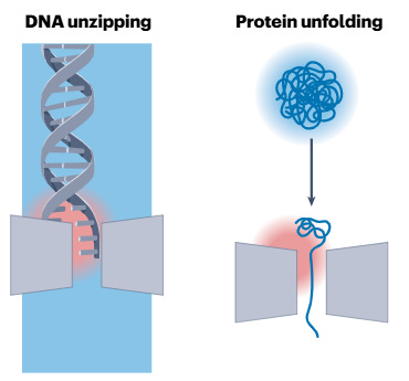
This paper explores how strategic temperature control could be used to unzip DNA/unfold proteins, without damaging the molecules.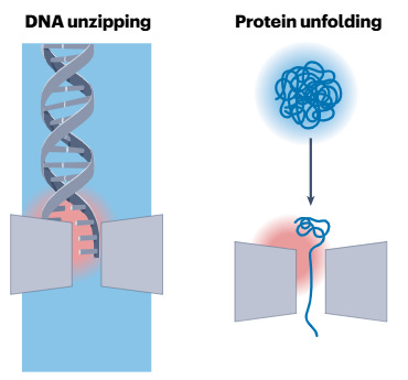
Figure 1: (a) Left - DNA being unzipped by increased temperature (b) Protein being unfolded by increased temperature in a solid state nanopore
Source: https://www.nature.com/articles/s44222-026-00485-9How long does it take for the molecule to pass through the pore?
DNA (and other biomolecules) pass through nanopores fairly quickly (microseconds), faster than any sensing system can deduce meaningful signals from it.
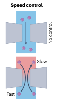
This paper recommends two temperature based approaches to slow down molecules passing through the pore:
i) local cooling in the nanopores can increase dwell times (time that a molecule hangs around in the pore) making it possible to get more snapshots of the molecule
ii) temperature gradients can cause DNA to expand and hence take longer to pass through the pore (similar to the expandomer approach that Roche’s new sequencer uses)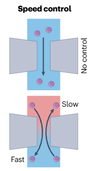
Figure 2: Controlling the speed of translocation (i.e. the process of a molecule moving from one side of the pore to the other)
Source: https://www.nature.com/articles/s44222-026-00485-9
3. Capture Rate
How do we get more of the same molecule to pass through the pore at a given time?
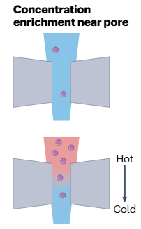
DNA moves from warmer to colder regions in a solution. This behaviour can be leveraged to enable the accumulation of a large concentration of DNA near the pore, thus enabling better detection.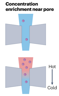
Figure 3: Enhancing capture rate through thermal gradient
Source: https://www.nature.com/articles/s44222-026-00485-9
4. Pore Sizes
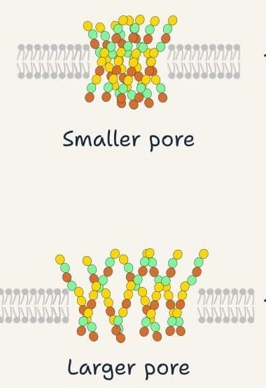
Size (i.e. diameter) is an important parameter of any nanopore system. It determines what kinds of molecules it can detect, and at what resolution.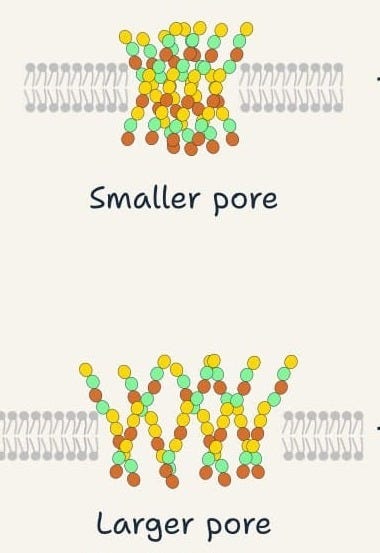
Figure 4: Illustration of pore sizes; Source: Plenty of Room
Pore sizes are usually only controllable during the pore fabrication process3 and it’s hard to get reliable sizes each time. The authors argue that temperature could be used to enlarge or shrink pore sizes, thus enabling size control at the device level post-fabrication.
5. The million dollar SNR4 question
Let’s first understand what kinds of noises typically show up in a solid state nanopore systems.
i) Johnson Nyquist Noise (also called Thermal Noise)
This noise arises from the intrinsic resistance of the electrolyte and the pore. It is frequency-independent (white noise) and sets a fundamental floor, proportional to temperature and inversely proportional to resistance (4kT/R). Lower pore/electrolyte resistance means lower thermal noise, but that trades off against signal amplitude.
ii) 1/f Noise (also called Flicker Noise)
This noise is attributed to surface charge fluctuations5 at the pore walls. It dominates below a crossover frequency that is typically in the 1–10 kHz range depending on the device; it’s especially problematic for slow measurements. Magnitude scales inversely with pore area and depends strongly on surface chemistry and passivation (coating on the surface of the membrane) quality.
(iii) Dielectric Noise
Nanopores are usually made on a membrane deposited on a support chip, for example silicon nitride membrane on a silicon chip. Dielectric noise comes from energy dissipation (loss) in the membrane/support chip material as they are not perfect insulators. It becomes significant at mid-to-high frequencies (i.e. 10 kHz to 90 kHz) and is sensitive to chip design.
(iv) Amplifier/Instrumentation Noise
An amplifier converts and boosts the tiny ionic current through the nanopore into a larger, measurable voltage signal. In nanopore setups, it also simultaneously applies and holds (”clamps”) the driving voltage across the membrane.
The current amplifier contributes voltage and current noise from its input stage electronics, independent of the pore/chip. As this stage handles the signal when it's at its smallest, any noise generated here gets added directly to the raw signal at its weakest point, and then gets amplified right along with the real signal by every subsequent stage. Noise introduced later in the amplification chain matters far less, since by that point the real signal has already been boosted well above it. Amplifier noise sets a baseline noise floor even with an ideal (infinite resistance, zero capacitance) pore.
(v) Capacitive Noise
Any two conductive surfaces (i.e. surfaces that allow electrons to pass through) separated by an insulator form a capacitor. In the context of a nanopore, like the electrolyte on either side of the silicon membrane, separated by the insulating membrane itself. When you apply a voltage across them, charge accumulates on each side. Capacitance (C) is a measure of how much electric charge a system can store for a given voltage applied across it.
Capacitive noise arises from the interaction between the amplifier’s input voltage noise and the total capacitance of the system. It scales with frequency squared, so dominates at high frequencies (100 kHz and above) and is the main bandwidth-limiting factor for fast single-molecule translocation measurements.
(vi) Shot Noise
Even at a perfectly steady, constant applied voltage, the exact number of ions passing through in any tiny time window fluctuates randomly. This randomness in the timing/count of individual charge-carrying events is what creates shot noise. It is usually negligible relative to other sources in typical nanopore conditions, though it can become relevant at very low ionic currents or very high bandwidths.
If we use temperature as a way to control the parameters listed above, do we not get more noise?
The authors suggest a few ways to get around this.
i. Ultra low capacitance device architectures
This includes reducing the size of the membrane (not the chip) on which the pore is made, thick insulating layers below and around the membrane, and fully insulating substrates (like glass) for the chip instead of silicon. Glass nanopores shows high SNR even at high temperatures.
ii. Post acquisition low pass filtering
A low-pass filter is a circuit that lets signals with a lower frequency than its cutoff pass through while reducing high-frequency signals.
iv. Engineer thermal environments in flow cells where the solid-state nanopore is kept between chemically inert heat-transfer fluids
v. Leverage on-chip, sub-micrometer thermometers6 that can measure nanoscale temperature variations and using it to construct a closed loop thermal feedback network that can be used to track pore destabilization due to thermal effects.
*****
This paper is largely theoretical. I would be keen to see how these approaches are tested experimentally. If you/someone in your network is testing these, I would love to chat.
*****
If you enjoyed reading this, two bonus articles to check out:
1. Data storage in DNA origami
2. DNA encryption inside cells
Victorian era version of the game Hot or Cold, where Player A hides an item and Player B has to find it; When B is close to the item A calls out hot, and when B is further away A calls out cold until B finds the item or runs out of time
https://www.nature.com/articles/s44222-026-00485-9
Which is done by TEM where a barrage of electrons are bombarded onto a chip, or UV lithography or controlled dielectric breakdown where a large electric field is applied to a small point on a chip causing it to break down)
Signal to Noise Ratio
surface charge fluctuations could be due to ion adsorption/desorption, trapping-detrapping of charges at defect sites in the membrane, and mobile surface charge dynamic
https://www.science.org/doi/10.1126/sciadv.abl7002